
Semiconductor-related technologies are attracting continuous attention as indispens-able basic technologies. In this research field, we aim to improve performance and break through technological limitations by introduc-ing new process new materials, new film deposition methods, and new structures to realize beyond 2nm advanced semiconductors.
Beyond 2nm new material process for advanced semiconductors and quantum devices
We are conducting the following research to realize beyond 2 nm advanced semiconductors by introducing new structures and materials.
- Interface engineering of new channel materials, including gate stack formation and work function control
- Fabrication technology for quantum devices such as superconducting qubits and silicon qubits
- New materials, new structural wiring and contact technology
Atomic layer process for fabrication of advanced nanodevices
We are conducting research on atomic-level processes and oxidation reactions for advanced nanodevices, such as atomic layer deposition and atomic layer etching.
- Atomic-level reaction analysis and processing deposition technology of semiconductor surfaces
- Understanding of oxidation mechanism of semiconductor surface and functional thin film
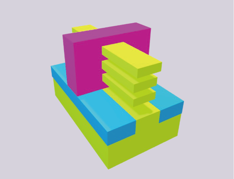 3D Nanosheet Transistor
 3D Nanosheet Transistor
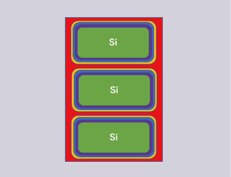
 Cross-section of Si nano-sheet
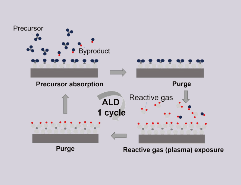 Schematic pictures of atomic layer deposition (ALD)
-
1 The study of ammonia combustion for carbon neutrality
-
2 Research and development of semiconductor nanodevices
-
3 Quantum/molecular dynamics analyses for the transport phenomena of materials in polymer electrolyte fuel cells
-
4 Development of ammonia combustion reaction models and its application to numerical combustion simulation