NEWS
ご挨拶
2022/11~ 研究室開設致しました
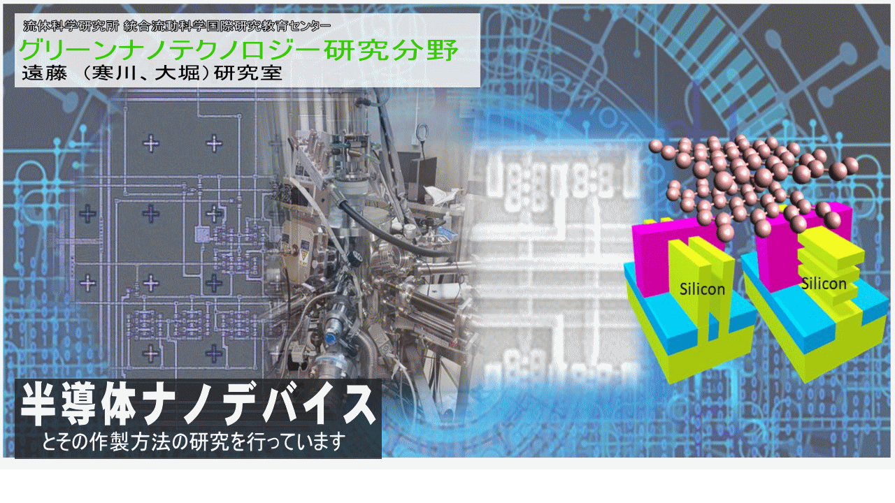
当研究室は、半導体技術で、情報やエネルギーの流れの制御を目指す研究室です。今や半導体関連技術は、我が国の経済安全保障上も非常に重要な技術とみなされる様になっております。この半導体技術の中でも、微細シリコンナノデバイスへの新プロセス・新材料・新規成膜手法・新構造導入による性能向上と技術限界の打破を目指します。
ナノデバイスをモチーフに置きながら、新物質、新材料・新構造の導入による、デバイスの超低消費電力化および高速化の技術限界の打破を目指して研究を行います。国内外オープンイノベーション拠点および産業界とも積極的に連携しながら研究を進めます。国内では、産業技術総合研究所(産総研・AIST)海外では、台湾国立陽明交通大学ジョイントラボリーを半導体デバイス開発の拠点として活用して参ります。台湾やアメリカ等に海外派遣のチャンスもあります。
Our laboratory aims to control the flow of information and energy using semiconductor technology. Semiconductor-related technology is now regarded as a very important technology for the economic security of our country. By using this semiconductor technology, we aim to improve performance and overcome technological limits by introducing new processes, new materials, new film formation methods, and new structures into fine silicon nanodevices. Using nanodevices as a motif, we aim to break through the technical limits of ultra-low power consumption and high speed devices. We will promote research while actively collaborating with domestic and overseas open innovation bases and industries. We will utilize the National Institute of Advanced Industrial Science and Technology (AIST/AIST) in Japan and the joint laboratory of Taiwan's Yang Ming Jiaotong University as bases for semiconductor device development overseas. There are also opportunities for overseas reesarch to Taiwan, the United States, etc.
学生の皆さんへ
2022年11月に開設された新しい研究室です。 研究室の立ち上げには、是非皆さんの力が必要です。半導体の分野で新しい研究室を一緒に立ち上げましょう。
本研究室は、グリーンナノテクノロジーの中でも、半導体ナノデバイスの研究を行います。半導体は、いまや生活に欠かすことのできない基幹デバイスです。半導体が無ければ自動車も製造できない状況を皆様もご覧になったことかと思います。ナノデバイスの寸法は、そのナノ通り、「ナノメートル」レベルで、ナノよりも更に微細な原子層レベルの材料制御を研究します。 半導体は、報道で示される通り、かつて日本がトップでしたが、この30年間ですっかり競争から脱落してしまいました。しかし、材料やプロセスでまだまだ日本が強い分野が残っているので、国内外の関連機関と連携しながら、日本の存在感を示していきたいと思います。半導体に興味のある方は、是非お話を聞きに来てください。 当研究室は、実際の実験による研究を行う研究室です。装置を組み上げたり、手作りすることもあります。就職後はどうしても既成装置を購入することになり、装置はブラックボックスになってしまいがちですが、大学では装置の中身を理解しながら実験に携わってもらいたいと考えております。 ゼミや実験、論文輪講などを通して、卒業するまでには、半導体の分野あるいはそれ以外の分野で活躍できる基礎知識を身に着けられます。海外留学や、外国学会への参加なども積極的に進めます。 ・機械工作が好きな人・海外(学会や留学)に行って見たい人・ナノの世界に憧れる人 是非見学に来てください。
This is a new laboratory opened in November 2022.
We need your help to set up our laboratory. Let's start a new laboratory
together in the field of semiconductors.
This laboratory conducts research on semiconductor nanodevices among green
nanotechnology. Semiconductors are core devices that are now indispensable
in our daily lives. I am sure that you have all seen the situation where
automobiles cannot be manufactured without semiconductors. The dimensions
of nanodevices study material control on an atomic layer-by-atom-layer
basis at the ``nanometer'' level. As reported in the media, Japan used
to be the leader in semiconductors, but over the past 30 years, it has
completely fallen out of the competition.However, there are still areas
where Japan is strong in materials and processes, so I would like to show
Japan's presence while collaborating with related organizations in Japan
and overseas. If you are interested in semiconductors, please come and
listen to us.
Our laboratory is a laboratory that conducts research through actual experiments.
You can build a device or make your own. After finding a job, it is inevitable
to purchase an existing device, and the device tends to be a black box,
but at the university, I would like you to understand the contents of the
device while participating in the experiment.
By the time you graduate, you will acquire basic knowledge that will enable
you to play an active role in the field of semiconductors and other fields
through seminars, experiments, and thesis lectures. We will actively promote
study abroad and participation in foreign academic conferences.
・People who like machine work ・People who want to go abroad (conferences
or study abroad) ・People who admire the nano world Please come and visit
us.