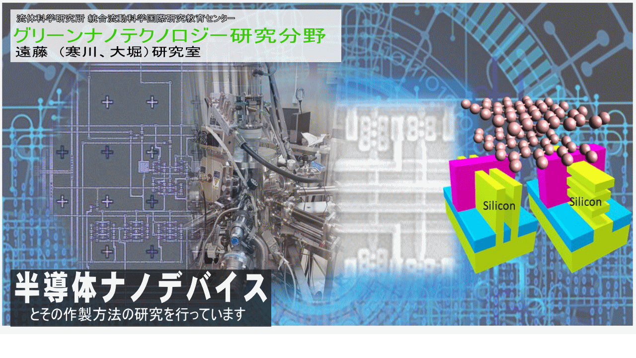
Research Topics
以下の研究を推進して参ります。
先端ナノデバイス作製のための原子層プロセス
・Atomic level processing for advanced nanodevices including atomic layer
etching and atomic layer deposition.
- Understanding atomic level reaction of semiconductor surfaces with
chemicals under energy controlled beams.
- New atomic level processing of semiconductor devices using new precursors
or new etching chemistry.
- Oxidation of semiconductor surfaces and functional thin films using
energy controlled oxygen beams.
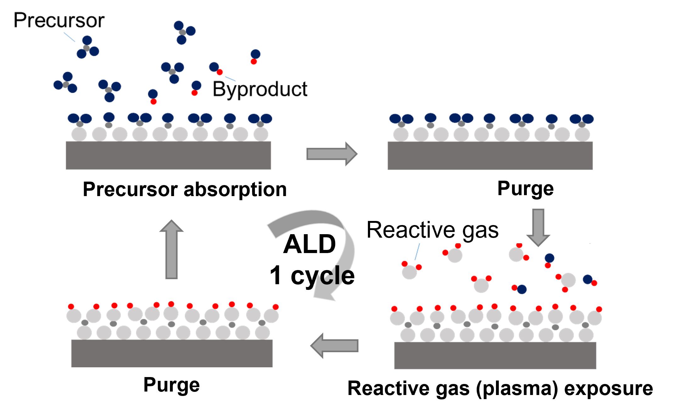
Atomic Layer Deposition (ALD) Process
先端ナノデバイスや量子デバイスのための新材料プロセス
・New materials and process technology for advanced nanodevices and quantum
devices.
- New channel materials including high mobility materials and 2D materials.
- Doping and contact issues for 2D materials.
- Interface engineering of new channel materials including gate stack
formation and work-function engineering.
- Damage free fabrication of quantum devices such as superconducting
qubits and silicon qubits.
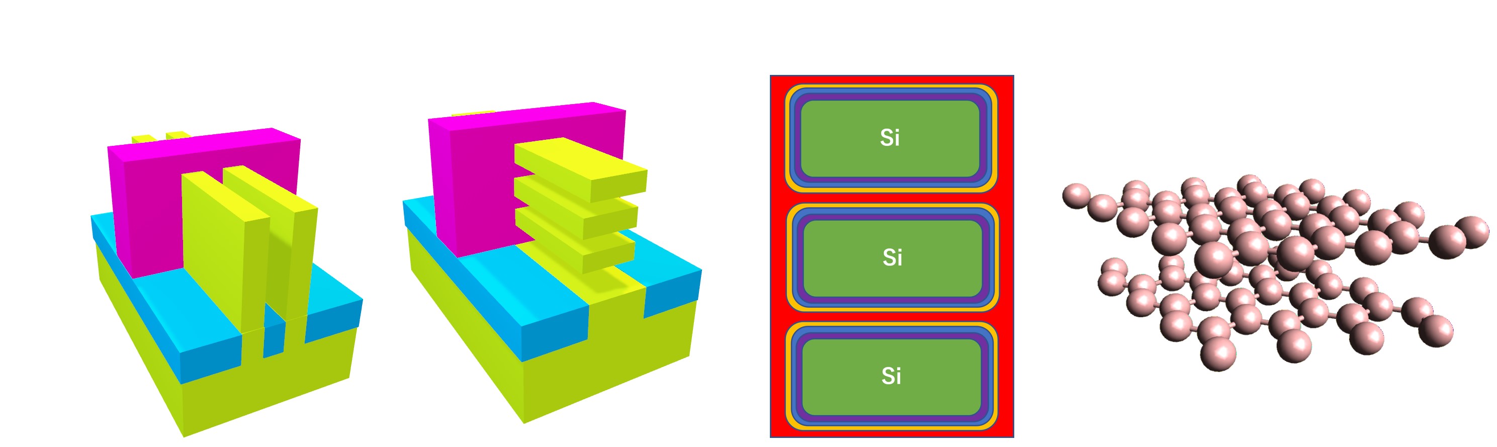
FinFET Nanosheet 2D Materials