研究テーマ
Newly Developed Neutral Beam Generation System
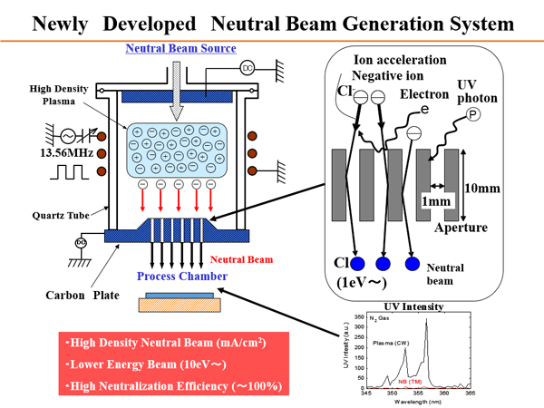
Neutral beam is an original technology of our laboratory [1-3]. It realizes ultimate damage-free processes for nano-devices such as etching, deposition, surface modification, oxidation, and so on.
Currently plasma process is widely used for fabrication of microdevices such as integrated circuits (IC). However, plasma causes damages to devices to be processed, because of irradiation of charged particles (ions) and UV/VUV photons. The charged particles causes differential charge-up on device and distortion of ion trajectories and etching profile. Also it may cause dielectric breakdown. High-density and high-energy UV/VUV photons radiating from plasma causes generation of high-density crystalline defects. These serious problems must be overcome in the fabrication of future nanoscale devices.
These problems are solved by neutral beam. It is generated from high density plasma. Ions in plasma are accelerated and collimated by electric field of the bottom electrode, and then they pass through the numerous high aspect ratio apertures at the bottom electrode. Ions are neutralized in high efficiency during the passage of the aperture, by collision of the aperture sidewall. As a result, collimated and energy-controlled beam of neutral particles can be obtained. Especially, when using halogen gases, application of pulse time modulation in the plasma source power enables generation of negative ions in the plasma [4], which enables almost 100% neutralization efficiency. Also, UV/VUV photon irradiation is suppressed by the aperture. As a result, it is possible to perform ultimate damage-free processes.
Neutral beam has been applied to various processes to prove its superior performance, such as gate etching of MOSFET [5], vertical fin channel fabrication in FinFET [6], low-temperature oxidation of silicon [7], neutral beam enhanced chemical vapor deposition [8], nanocolumn and quantum dot fabrication combined with bio-template technique [9,10], modification of organic molecule monolayer [11], carbon nanotube transistor [11], microelectromechanical systems (MEMS) [12], and so on. Now neutral beam is our foundation technology to develop various future nanodevices.
Besides experimental studies, theoretical calculation is also performed. The neutralization process by collision of ions against aperture surface was calculated based on time-dependent density functional theory [13]. Neutralization mechanisms of positive and negative ions were investigated.
- [1]
- Seiji Samukawa, Keisuke Sakamoto and Katsunori Ichiki, High-performance Neutral Beam Generation using Inductively Coupled Plasma, Japanese Journal of Applied Physics, Vol. 40 (2001) pp. L779-L782. <http://dx.doi.org/10.1143/JJAP.40.L779>
- [2]
- Seiji Samukawa, Keisuke Sakamoto and Katsunori Ichiki, High-Efficiency Low Energy Neutral Beam Generation Using Negative Ions in Pulsed Plasma, Japanese Journal of Applied Physics, Vol. 40 (2001) pp. L997-L999. <http://dx.doi.org/10.1143/JJAP.40.L997>
- [3]
- Seiji Samukawa, Keisuke Sakamoto and Katsunori Ichiki, Generating High-efficiency Neutral Beams by Using Negative Ions in an Inductively Coupled Plasma Source, Journal of Vacuum Science and Technology A, Vol. 20 (2002) pp. 1566-1573. <http://dx.doi.org/10.1116/1.1494820>
- [4]
- Hiroto Ohtake and Seiji Samukawa, Charge-free etching using both positive and negative ions in pulse-time modulated ECR plasma with low frequency bias, Applied Physics Letters, Vol. 68 (1996) pp. 2416-2417. <http://dx.doi.org/10.1063/1.116152>
- [5]
- Shuichi Noda, Hiromoto Nishimori, Tohru Iida, Tsunetoshi Arikado, Katsunori Ichiki, Takuya Ozaki and Seiji Samukawa, 50nm Gate Electrode Patterning Using A Neutral-Beam Etching System, Journal of Vacuum Science and Technology A, Vol. 22 (2004) pp. 1506-1512. <http://dx.doi.org/10.1116/1.1723338>
- [6]
- Kazuhiko Endo, Shuichi Noda, Meishoku Masahara, Tomohiro Kubota, Takuya Ozaki, Seiji Samukawa, Yongxun Liu, Kenichi Ishii, Yuki Ishikawa, Etsuro Sugimata, Takashi Matsukawa, Hidenori Takashima, Hiromi Yamauchi, and Eiichi Suzuki, Fabrication of FinFET by Damage-free Neutral Beam Etching Technology, IEEE Transactions on Electron Devices, Vol. 53 (2006) pp. 1826-1833. <http://dx.doi.org/10.1109/TED.2006.877035>
- [7]
- Masahiro Yonemoto, Keisuke Sano, Kazuhiko Endo, Takashi Matsukawa, Meishoku Masahara and Seiji Samukawa, Low temperature, Beam-Orientation-Dependent, Lattice-Plane-Independent, and Damage-Free Oxidation for Three-Dimensional Structure by Neutral Beam Oxidation, Japanese Journal of Applied Physics, Vol. 48 (2009) pp. 04C007 (5pp). <http://dx.doi.org/10.1143/JJAP.48.04C007>
- [8]
- Shigeo Yasuhara, Juhyun Chung, Kunitoshi Tajima, Hisashi Yano, Shingo Kadomura, Masaki Yoshimaru, Noriaki Matsunaga, Tomohiro Kubota, Hiroto Ohtake and Seiji Samukawa, Structure-designable method to form super low-k SiOC film (k = 2.2) by neutral-beam-enhanced chemical vapor deposition, Journal of Physics D: Applied Physics, Vol. 42 (2009) pp. 055208 (7pp). <http://dx.doi.org/10.1088/0022-3727/42/5/055208>
- [9]
- Tomohiro Kubota, Tomohiro Baba, Hiroyuki Kawashima, Yukiharu Uraoka, Takashi Fuyuki, Ichiro Yamashita and Seiji Samukawa, A 7nm-Nanocolum Structure Fabricated by Using a Ferritin Iron-Core Mask and Low Energy Cl Neutral Beams, Applied Physics Letters, Vol. 84 (2004) pp. 1555-1557. <http://dx.doi.org/10.1063/1.1655701>
- [10]
- Tomohiro Kubota, Takeshi Hashimoto, Yasushi Ishikawa, Seiji Samukawa, Atsushi Miura, Yukiharu Uraoka, Takashi Fuyuki, Masaki Takeguchi, Kensuke Nishioka, and Ichiro Yamashita, Charging and Coulomb staircase effects in silicon nanodisk structures fabricated by defect-free Cl neutral beam etching process, Applied Physics Letters, Vol. 89 (2006) pp. 233127 (pp). <http://dx.doi.org/10.1063/1.2404608>
- [11]
- Seiji Samukawa, Yasushi Ishikawa, Keiji Okumura, Yoshinori Sato, Kazuyuki Tohji and Takao Ishida, Damage-free Surface Treatment of Carbon Nanotube and Self-assembled Mono-layer Devices Using a Neutral-Beam Process for Fusing Top-down and Bottom-up Processes, Journal of Physics D: Applied Physics, Vol. 41 (2008) pp. 024006 (6pp). <http://dx.doi.org/10.1088/0022-3727/41/2/024006>
- [12]
- Maju Tomura, Chi-Hsien Huang, Yusuke Yoshida, Takahito Ono, Satoshi Yamasaki, and Seiji Samukawa, Plasma-Induced Deterioration of Mechanical Characteristics of Microcantilever, Japanese Journal of Applied Physics, Vol. 49 (2010) pp. 04DL20 (4pp). <http://dx.doi.org/10.1143/JJAP.49.04DL20>
- [13]
- Tomohiro Kubota, Naoki Watanabe, Shingo Ohtsuka, Takuya Iwasaki, Kohei Ono, Yasuroh Iriye, and Seiji Samukawa, Numerical simulation on neutral beam generation mechanism by collision of positive and negative chlorine ions with graphite surface, Journal of Physics D: Applied Physics, Vol. 44 (2011) pp. 125203 (5pp). <http://dx.doi.org/10.1088/0022-3727/44/12/125203>
Contents
- Newly Developed Neutral Beam Generation System
- Silicon Quantum Dot Solar Cell
- Surface investigation of III-V compound
- Quantum Dot Solar Cell (Ge)
- Optics application of III-V compound nano dot
- Fabrication of graphene
- Ultrathin Oxide Film for Nanodevices
- Conductive DLC film synthesis by NBECVD technique and its application as sensor of Bio-LSI


