研究テーマ
Staff (as for fiscal year 2014):
Ass. Prof. Higo A.
Dr. Thomas C.
Goal for making III-V nanopillars embedding quantum dots
Quantum dot (QD) lasers are one of the most promising light sources because of their theoretically improved performance compared to quantum well and bulk lasers [1]. Due to the change in the density of states caused by the three-dimensional confinement, QD lasers are expected to have high temperature stability [2], low threshold currents [3], and large modulation band width [4]. These QDs are usually formed from molecular beam epitaxy (MBE) methods. Namely, Stranski-Krastanov growth mode is used to form strained islands that develop into high-quality crystals without any process-induced damage. However this narrows the useful materials for making NDs as a lattice-mismatched system is required. For optoelectronic devices, it has been demonstrated that QD active layers can enhance the optical gain. When high-density, high-uniformity, and multiply-stacked QDs layers conditions were fulfilled, large optical gain would be obtained. But it is still a great challenge to achieve all these conditions. Therefore, we have investigated a top-down approach for the fabrication of QDs, by combining a bio-nano-process (BNP) [5] and a damage-free, neutral beam etching (NBE) process [6]. In this work, we report recent results obtained on the fabrication of InGaAs NDs embedded in a GaAs barrier layer and their optical characteristics.
Method used
Multi-quantum well samples (MQW) were grown by metalorganic vapor phase epitaxy (MOVPE), as shown in Fig. 1(a). After conventional organic cleaning of the surface, a self-assembled monolayer of PEGylated ferritins (cage-liked proteins with an outer diameter of 13 nm and an inner diameter of 7 nm in which an iron oxide core of 7 nm can be introduced) was formed (Fig. 1(b)) [5]. Protein shells were then removed by low-temperature oxygen annealing in vacuum (LT-OAV) leaving the metal oxide cores on the surface as etching mask, Fig. 1(c). Afterwards, the surface oxide layer was removed by hydrogen radical treatment using an ECR gun at 350 °C and surface was passivated by flowing hydrogen radicals at room temperature. Chlorine neutral beam etching was subsequently carried out using a flow rate of 40 sccm and an ICP power of 800 W. Substrate temperature as well as beam energy effects on etching nanostructures were investigated. After NBE, hydrogen radical treatment was performed to passivate the surface. Afterwards, iron oxide cores were removed and barrier layer was regrown by MOVPE. Finally, photoluminescence spectra were measured to observe the quantum confinement effect of the fabricated NDs.
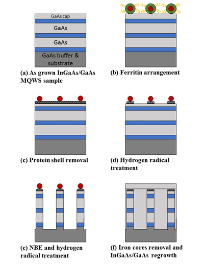
Figure 1 Process flow of nanodisks fabrication. (a) MOVPE as-grown InGaAs/GaAs MQWs sample, (b) PEG-ferritin arrangement, (c) removal of protein shell by LT-OAV, (d) surface oxide removal by hydrogen radical, (e) etching by neutral beam and passivation by hydrogen, (f) removal of iron cores and regrowth of barrier
References
- [1]
- Y. Arakawa and H. Sakaki, Appl. Phys. Lett., 40 (1982) 939.
- [2]
- M. Asada, Y. Miyamoto and Suematsu Y., IEEE J. Quantum Electron., 22 (1986) 1915.
- [3]
- D. Bimberg, N. Kirstaedter, N.N. Ledentsov, Zh.I. Alferov.P.S. Kop'ev and V.M. Ustinov, IEEE J. Sel. Top. Quant., 3 (1997) 196.
- [4]
- R. Mirin, A. Gossin, and J. Bowers, Electron. Lett., 32 (1996) 1732.
- [5]
- I. Yamashita, Thin Solid Films, 393 (2001) 12.
Publications:
[1] Xuan-Yu Wang, Chi-Hsien Huang, Yuzo Ohno, Makoto Igarashi, Akihiro Murayama, and Seiji Samukawa, Defect-free etching process for GaAs/AlGaAs hetero-nanostructure using chlorine/argon mixed neutral beam, Journal of Vacuum Science and Technology B, Vol. 28 (2010) pp. 1138-1142, IF=1.358.
[2] Xuan-Yu Wang, Chi-Hsien Huang, Rikako Tsukamoto, Pierre-Andre Mortemousque, Kohei M Itoh, Yuzo Ohno, and Seiji Samukawa, Damage-free top-down processes for fabricating two-dimensional arrays of 7 nm GaAs nanodiscs using bio-templates and neutral beam etching, Nanotechnology, Vol. 22 (2011) pp. 365301 (9pp), IF=3.672.
[3] Yosuke Tamura, Toshiyuki Kaizu, Takayuki Kiba, Makoto Igarashi, Rikako Tsukamoto, Akio Higo, Weiguo Hu, Cedric Thomas, Mohd Erman Fauzi, Takuya Hoshii, Ichiro Yamashita, Yoshitaka Okada, Akihiro Murayama and Seiji Samukawa, Quantum size effects in GaAs nanodisks fabricated using a combination of the bio-template technique and neutral beam etching, Nanotechnology, Vol. 24 (2013) pp. 285301 (6pp), IF=3.672.
[4] Cedric Thomas, Yosuke Tamura, Mohd Erman Syazwan, Akio Higo, and Seiji Samukawa, Oxidation states of GaAs surface and their effects on neutral beam etching during nanopillar fabrication, Journal of Physics D: Applied Physics, Vol. 47 (2014) pp. 215203 (11pp), IF=2.521.
[5] Cedric Thomas, Yosuke Tamura, Takeru Okada, Akio Higo and Seiji Samukawa, Estimation of activation energy and surface reaction mechanism of chlorine neutral beam etching of GaAs for nanostructure fabrication, Journal of Physics D: Applied Physics, Vol. 47 (2014) pp. 275201 (7pp), IF=2.521.
Contents
- Newly Developed Neutral Beam Generation System
- Silicon Quantum Dot Solar Cell
- Surface investigation of III-V compound
- Quantum Dot Solar Cell (Ge)
- Optics application of III-V compound nano dot
- Fabrication of graphene
- Ultrathin Oxide Film for Nanodevices
- Conductive DLC film synthesis by NBECVD technique and its application as sensor of Bio-LSI


