研究テーマ
Fabrication of graphene
Fabrication of nano graphene by neutral beam is now carrying on without generating undesirable defect at the edge.
Extremely low damage neutral beam etching is applied to graphene nano ribbon fabrication. The graphene nano ribbons are fabricated by electron beam lithography followed by oxygen neutral beam from CVD grown graphene.
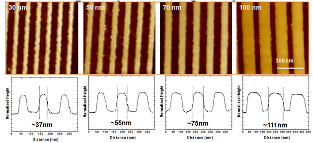
AFM images of Graphene nanoribbons fabricated by neutral beam etching
Figure 1 shows AFM images and profiles of graphene nano ribbon arrays with various widths. We can clearly see that the widths of the graphene nano ribbon arrays are close to the same size as the patterns by electron beam lithography. The images and figures exhibit uniform patterning.
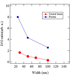
Raman D/G ratio.
Figure 2 indicates that representative Raman spectra of graphene nano ribbon arrays with various widths. Ratio of integrated intensities of the D- and G-band are plotted as a function of the width. The ratio of D/G band intensity is the indicator of the defect level at the edge. The ratio increases as the width decreases, however, the ratio is impressively lower than that of the ribbons fabricated by conventional plasma etching. Ever if graphene is covered with resist mask, UV irradiation induces defect generation, which is isotropic irradiation from plasma.
We have demonstrated graphene nano ribbon arrays fabrication by neutral beam etching. Neutral beam system can provide low energy and energy-controlled neutral beams without UV irradiation damage, so it is possible to high quality graphene nano ribbon arrays, which can be applied for field effect transistor.
Contents
- Newly Developed Neutral Beam Generation System
- Silicon Quantum Dot Solar Cell
- Surface investigation of III-V compound
- Quantum Dot Solar Cell (Ge)
- Optics application of III-V compound nano dot
- Fabrication of graphene
- Ultrathin Oxide Film for Nanodevices
- Conductive DLC film synthesis by NBECVD technique and its application as sensor of Bio-LSI


